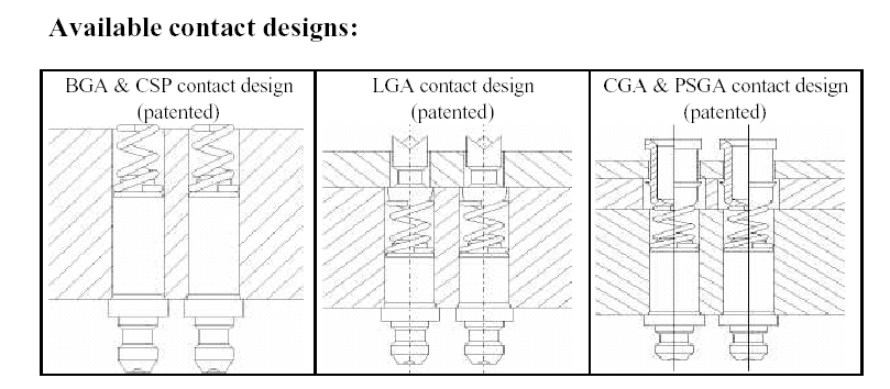
Patented socketing system for the BGA/CSP technology
Features: ¨ ZIF handling & only 40 grams per contact after
closing the socket
¨ Sockets adapt to all package styles (at present down to 0.75mm pitch):
Ceramic & plastic BGA (cavity up & down), CSP, LGA, CGA, PSGA
¨ Same PCB layout as the chip (no holes required for SMD socket)
¨ Raised SMD for lifting socket over components
¨ Thermal expansion, shock & vibration absorbed by JSI contact design
¨ Low profile socket (standard screw lock is less than 10mm with chip)
¨ Heat dissipation with open frame or heatsinks
¨ Low inductance of less than 5 nH
¨ Frequency range up to 400 Mhz
¨ LGA contact design can also be used for board-to-board connections
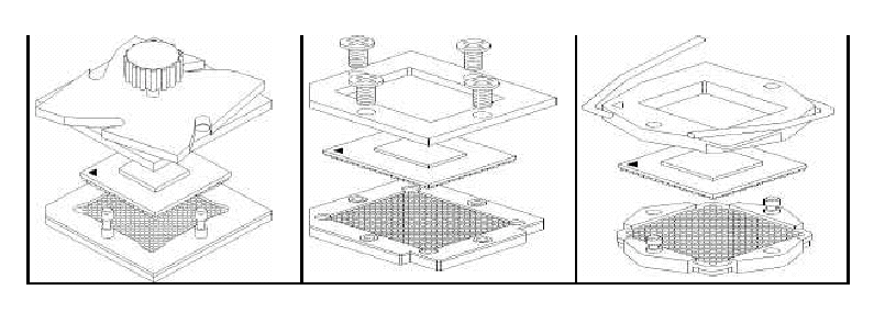
Available retention designs:
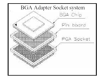
Alternative BGA socket = Adapter system:
Advantages:
smaller outer dimensions than true socket
Disadvantages:
Chip needs to be soldered to adapter board
Can only be used with BGA chips
Smallest pitch is 1.00mm
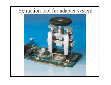
Relatively high insertion & extraction forces (difficult without tool)
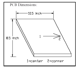
Recommended Solder profile (hot air convection method):
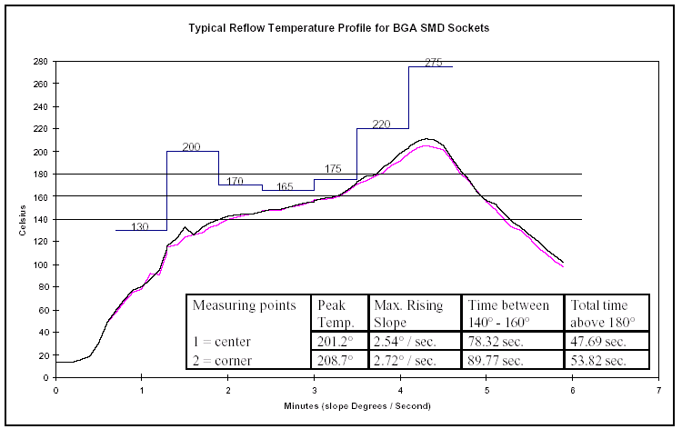
Solder Paste = Alpha Metals WS619
Solder paste Thickness = 6 - 7.5 Mils
Belt Speed = 25 Inch / min
BTU Oven ( hot air convection )
4
Chip package styles used with JSI sockets:
BGA “Ball Grid Array”
Comprises plastic packages with “cavity up” (= processor is located on top of
the
substrate) and “cavity down” (= processor is located below the substrate), as
well as
ceramic packages. The plastic packages with 1.27mm ball pitch have solderballs
of
0.60mm (.024 inch) height with a diameter of 0.76mm (.030 inch), while the ceramic
packages have solderballs of 0.90mm (.035 inch) height with a diameter of 0.86
(.034
inch). The most common pitch is 1.27mm (.050 inch), but other pitches such as
1.00mm
(.039 inch), 1.50mm (.059 inch) or 2.00mm (.079 inch) or interstitial pitches
are also
available.
CSP “Chip Scale Packaging”
The outer dimensions of these packages, which are also supplied in “ball grid
array
technology”, are designed so as not to exceed the size of the processor by more
than 20%.
The pitch starts with 0.80mm (.032 inch) and reduces to 0.50mm (.020 inch).
The
solderball diameter in this pitch size is as little as 0.30mm (.012 inch).
LGA “Land Grid Array”
These chips are supplied with a gold pad (= land) instead of the solderballs.
The advantage
of this package is that it is cheaper to manufacture (no solder balls required).
The
disadvantage is that it is more difficult to assemble onto a PCB (connector
required).
CGA “Column Grid Array”
Soldercolumns of more than 2.00mm (.079 inch) height replace the standard 0.90mm
(.035 inch) solderballs. These soldercolumns overcome the problem of “thermal
expansion” of the chip and the inherent mechanical stress this exercises on
the solderjoints
of standard solderballs. These relatively soft columns have the ability of absorbing
the
“micro movements” of the chip thus eliminating the problem.
PSGA “Plastic Stud Grid Array”
This new packaging technology has been developed jointly by the “Inter-University
Microelectronics Center” and the “Laboratory for Production Technology of Siemens”
in

Belgium. It offers “gold plated plastic studs” instead of solderballs and the
height is also
very low (1.50mm to 2.00mm, resp. .059 inch to .079 inch). The studs are presently
available in an interstitial pitch of 1.00mm (.039 inch).
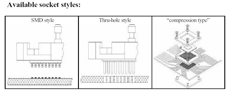
Screw lock type -ZIF lever lock type- Knob lock type Solderless compression type ............Footprints: 1.27mm pitch - 1.00mm pitch - 0.80mm pitch -............. special footprints Special info - Tool
경기도 안양시 동안구 호계 1동 555-9, 안양 유통상가 17동 127호
Tel 031-479-4211/2
Fax 031-479-4213
JSi@JSiTS.com
JS Engineering Co.
yourmook@lycos.co.kr